
Key insights:
- Most of the semiconductor industry’s raw materials risk stems from supply concentration, rather than physical scarcity, where they are often sourced from only a few countries or regions.
Supply concentration risks can be further hampered by elevated geopolitical risks, where, for example, Africa and China supply approximately 70% of tantalum and silicon globally, which are widely used in semiconductor manufacturing.
- Initiatives to increase the share of reused or recycled materials in manufactured products can alleviate sourcing risks by reducing the need for virgin raw materials, however, these initiatives do not fully replace raw material inputs.
The widespread adoption of emerging computing applications, such as autonomous vehicles, artificial intelligence and 5G communication technology, is significantly boosting demand for semiconductors. Demand for their underlying raw materials is therefore expected to also rise.¹ As the semiconductor industry encounters the physical limitations of transistor density and chip size, its fabs are turning to alternative raw materials. These material inputs sustain advances in processing power² or advanced production methods that require more processing steps and entail higher consumption of process gases³ and packaging materials. That said, exponential demand for semiconductors is not the sole factor underpinning potential resource strain.⁴
Supply Concentration and Geopolitical Risks: Raw Materials
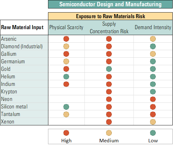
Raw materials used by the semiconductor industry are often sourced from only a few countries or regions. As part of the recent enhancements to our ESG Risk Ratings, Morningstar Sustainalytics’ new material ESG issue (MEI) on Raw Materials Use shows that most of the semiconductor industry’s raw materials risk stems from supply concentration, rather than physical scarcity (see Tables 1 and 2). Raw materials used by the semiconductor industry are often sourced from only a few countries or regions.
Table 1. Summary of Semiconductor Design and Manufacturing Raw Materials Risk by Input
Source: Morningstar Sustainalytics. For informational purposes only.
Note: Data as of December 2023. Based on data from United States Geological Survey (USGS), Eurostat, International Energy Agency (IEA), Sustainalytics Institutional Capital Scores, and other Sustainalytics research. Risk categories of physical scarcity, supply concentration risk and demand intensity are expressed by the categories High, Medium or Low.
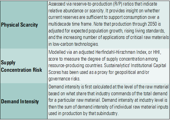
Table 2. Description of Risk Drivers for Raw Materials Use Exposure
Source: Morningstar Sustainalytics. For informational purposes only.
Supply concentration risks can be made worse by elevated geopolitical risks. For example, Africa (where there are risks from political instability, corruption, or conflicts) and China (where there are risks from trade disputes and export bans) supply approximately 70% of tantalum and silicon globally⁵ – two materials widely used in semiconductor manufacturing. The pandemic also highlighted underlying supply chain vulnerabilities, which were further amplified for raw materials with a high geographic concentration.
Supply Concentration and Geopolitical Risks: Process Gasses
We assess risks of the various raw materials used in semiconductor end-products and in those required during the manufacturing process, including process gases. Process gases are ubiquitous across the semiconductor manufacturing process due to their function as agents for cooling or to provide an inert environment (e.g., helium). They are also used to modulate the innate properties⁶ of semiconductors via doping (arsine), etching, annealing and deposition (e.g., krypton, xenon). Neon is the main component of laser gas, which is used during the photolithographic process to pattern semiconductors. During this process, parts of the substrate, typically a silicon wafer, are selectively exposed to ultraviolet light, creating a chemical reaction that transfers a pattern onto the wafer.
The semiconductor industry accounts for the majority of global demand for neon, which is a byproduct of steel production.⁷ To avoid cross-contamination and unwanted impurities, these process gases must be ultra-pure.
Roughly half of semiconductor-grade neon supply was disrupted following Russia’s invasion of Ukraine, as Ukrainian suppliers shuttered their operations.⁸ While Russia is a dominant supplier of crude neon, the purification process tends to take place in Ukraine. Export restrictions and economic sanctions imposed on Russia further tightened supply. These examples underscore the geographically concentrated nature of specific raw materials and how supply chain vulnerabilities can rapidly form bottlenecks that may force semiconductor fabs to halt or curtail production.
Although geographic diversification of raw material supply lines can alleviate vulnerabilities, some raw materials have few alternatives; e.g., 98% of raw gallium is supplied by China.⁹ Another tactical approach to mitigate supply volatility is to build up raw materials inventory to act as a buffer, which occurred through 2021.¹⁰ Other methods may be preferred, though, as stockpiling can result in excessive inventory holding costs. Selecting the most effective method can be difficult. A single raw material may play multiple roles, where hidden supply bottlenecks may emerge at various stages of the manufacturing process (see Table 3).
Table 3. Application Examples of Raw Material Inputs for Semiconductors
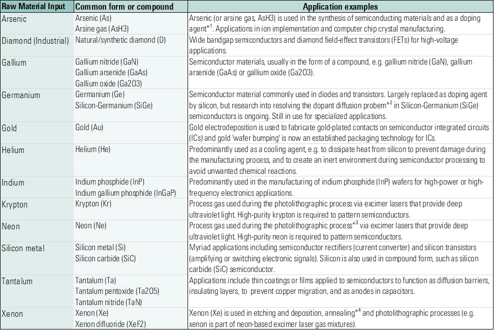
Source: Morningstar Sustainalytics. For informational purposes only.
Notes:
*¹ Doping is the intentional introduction of impurities into an (undoped) semiconductor for the purpose of altering its electrical, optical, and structural properties.
*² Dopant diffusion problem refers different diffusion rates in germanium-based alloys compared to pure silicon. Dopant diffusion is the movement of impurity atoms (dopants) within a semiconductor material to affect its innate properties at high temperatures.
*³ Photolithographic process uses light, typically ultraviolet (UV), to transfer a pattern onto a substrate (usually a silicon wafer) that has a photosensitive surface.
*⁴ Annealing is a heat treatment process that alters the physical and sometimes chemical properties of a material to increase its ductility and reduce its hardness.
Various Management Approaches to Address Risk
Initiatives to increase the share of reused or recycled materials in manufactured products can alleviate sourcing risks by reducing the need for virgin raw materials.¹¹ However, these initiatives do not fully replace raw material inputs, and their effectiveness depends on the raw materials in scope. As the focus of semiconductor fabs is on byproducts and processing materials, rather than on direct raw material inputs, this management strategy is at an early stage.
Another strategy among several semiconductor fabs is to implement end-of-life product stewardship programs. The programs are focused on ‘waste-to-X’ initiatives to valorize waste (by-)products (i.e., find ways of reusing, recycling, or converting them), rather than on traditional take-back programs, since semiconductors are rarely sold directly to end-consumers by pure-play manufacturers. These technologies are in their infancy and do not generally focus on raw materials reclamation to reduce sourcing risks.
More mature management strategies, such as eco-design, also entail circularity and resource conservation considerations to minimize the environmental impact of a product across its life cycle. Although the bulk of eco-design initiatives focus on the product use phase among semiconductor fabs, product design that also considers procurement and a manufacturing process that preserves raw materials form a more holistic approach. By identifying raw materials with high sourcing risks and optimizing, substituting, or phasing out their use, companies can effectively reduce their need for virgin materials.
Innovation programs for raw materials may involve implementing new production technologies that can cut raw material use, or finding viable substitutes to replace high-risk raw materials with more sustainable alternatives for which sourcing risks are lower. Emerging research on alternative materials in the semiconductor industry ranges from biobased mimetic materials to carbon nanotubes, or hybrid-materials. Effective substitutes may avoid silicon’s thermal conductivity problem (i.e. silicon’s ability to conduct heat diminishes in tandem with chip size),¹² and simultaneously bolster a company’s supply chain, or even result in a competitive advantage if leveraged correctly. However, these are nascent technologies, and achieving scalability and economic viability may prove tricky. Companies may need to line up potential substitutes for scarce or supply-concentrated raw materials to avoid supply chain issues over the next few decades.
Companies can minimize supply chain vulnerabilities through a combination of management strategies, including geographic diversification of raw materials sourcing (where possible), and initiatives that underpin circularity. Semiconductor materials are selected based on innate characteristics, such as thermal conductivity or optical transparency; therefore, alternative materials cannot be applied indiscriminately, as they often do not match the original material’s characteristics. While future technological advances offer possibilities (e.g., organic semiconductor materials and ultra-low temperature manufacturing),¹³ at present, there is no single solution for semiconductor fabs to entirely prevent raw materials risks.
References
- FPT Semiconductor. 2024. “Overview of the Semiconductor Raw Materials Industry”. FPT Semiconductor. March 7, 2024. https://fpt-semiconductor.com/blogs/overview-of-the-semiconductor-raw-materials-industry/
- Murphy, M. 2022. “The path to 1 nanometer chips and beyond.” IBM. December 5, 2022. https://research.ibm.com/blog/1nm-chips-vtfet-ruthenium
- Tembey, G. Sexton, T. Richard, C. Palma, R. Mohr, J. 2023. “A Net Zero Plan for the Semiconductor Industry.” Boston Consulting Group. September 12, 2023. https://www.bcg.com/publications/2023/a-plan-to-reduce-semiconductor-emissions#:~:text=Manufacturing%20more%20advanced%20semiconductors%20requires%20ever%20more%20complex,coming%20years%20and%20not%20peak%20until%20about%202045
- Mohammad, W. Elomri, A. Kerbache, L. 2022. “The Global Semiconductor Chip Shortage: Causes, Implications, and Potential Remedies.” International Federation of Automatic Control (IFAC). October 26, 2022. https://www.sciencedirect.com/science/article/pii/S2405896322017293
- According to Sustainalytics research and data from United States Geological Survey.
- Innate properties encompass the electrical, chemical, optical, or structural properties of semiconductors, for more information see: Gupta, K.M. Gupta, N. 2015. “Semiconductor Materials: Their Properties, Applications, and Recent Advances.” Advanced Semiconducting Materials and Devices. January 1, 2015. https://doi.org/10.1007/978-3-319-19758-6_1
- Fukuda, H. 2016. “Chipmakers seek solution to neon gas supply shortage.” Semiconductor Digest. March 2016. https://sst.semiconductor-digest.com/2016/03/chipmakers-seek-solution-to-neon-gas-supply-shortage/
- Alper. A. 2022. “Exclusive: Russia’s Attack on Ukraine Halts Half of World’s Neon Output for Chips.” Reuters. March 11, 2022. https://www.reuters.com/technology/exclusive-ukraine-halts-half-worlds-neon-output-chips-clouding-outlook-2022-03-11/
- Funaiole, M.P. Hart, B. Powers-Riggs, A. 2023. “Mineral Monopoly: China’s Control over Gallium Is a National Security Threat.” Center for Strategic and International Studies (CSIS). August 3, 2023. https://csis-website-prod.s3.amazonaws.com/s3fs-public/2023-08/230803_Funaiole_GalliumSupplyChains.pdf?VersionId=PivHd2uZ06pXG_STA__k6zihayX9iObn
- Klotz, A. 2021. “Chip Manufacturers Stockpile Record Amount of Raw Materials to End Shortage.” Tom’s Hardware. August 23, 2021. https://www.tomshardware.com/news/chip-makers-stockpile-record-amount-of-raw-materials#:~:text=As%20reported%20by%20Nikkei%20Asia%2C%20the%20world%27s%20nine,Digital%2C%20and%20more%2C%20is%20now%20at%20historic%20highs.
- Measured by the management indicators ‘recycled material use’ and ‘recycled material programs.’
- Pernot et al. 2023. “A Review of Nano and Microscale Heat Transfer: An Experimental and Molecular Dynamics Perspective.” Nature Materials. September 12, 2023. https://www.mdpi.com/2227-9717/11/9/2769
- Torricelli, F. Alessandri, I. Macchia, E. Vassalini, I. Maddaloni, M. Torsi, L. 2021. “Green Materials and Technologies for Sustainable Organic Transistors.” Advanced Materials Technologies. July 28, 2021. https://onlinelibrary.wiley.com/doi/10.1002/admt.202100445


